 Image: intelligentliving.co
As artificial intelligence workloads continue to explode the demand for power in data centers, Intel Foundry is delivering a timely innovation that could reshape power delivery and chip design. On April 9, 2026, the company announced the world's thinnest gallium nitride (GaN) chiplet technology, with a silicon substrate thinned to a mere 19 micrometers—roughly one-fifth the width of a human hair. Built on 300mm GaN-on-silicon wafers, this breakthrough integrates high-performance GaN power transistors with silicon-based digital control logic on a single monolithic die. Presented at the 2025 IEEE International Electron Devices Meeting (IEDM), the development signals Intel's aggressive push into advanced heterogeneous integration as part of its 'Systems Foundry' strategy for the AI era.
This isn't just another incremental improvement in semiconductor tech. By bringing power electronics and digital intelligence together in an ultra-compact form factor, Intel Foundry is addressing one of the biggest bottlenecks in modern computing: efficient, high-density power delivery close to the processor. With GaN's superior switching speeds, voltage handling, and thermal properties compared to traditional silicon, this chiplet technology could slash energy losses, reduce cooling requirements, and enable smaller, more powerful systems across AI accelerators, servers, 5G/6G infrastructure, and beyond.
The Technical Breakthrough: Ultra-Thin GaN Meets Monolithic Integration
At the heart of Intel Foundry's announcement is a first-of-its-kind manufacturing achievement. Engineers successfully fabricated GaN devices on standard 300mm silicon wafers, then employed a proprietary stealth dicing before grinding (SDBG) process to thin the silicon base to just 19μm without damaging the active structures. This extreme thinning enables the chiplet to be integrated into advanced packaging schemes with minimal height, ideal for 2.5D and 3D heterogeneous designs.
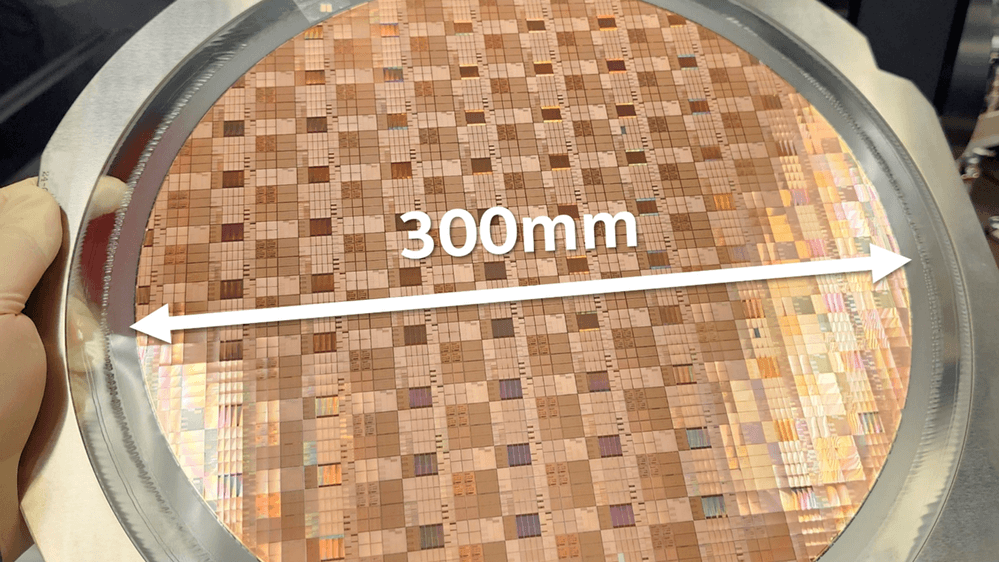 Image: 3dincites.com
What truly sets this apart is the monolithic integration. Traditionally, GaN power devices and silicon logic circuits have been manufactured separately due to material and process incompatibilities. Intel's approach combines GaN N-channel MOSHEMT (metal-oxide-semiconductor high-electron-mobility transistors) for power handling with silicon PMOS transistors for digital logic using a layer transfer technique—all on the same wafer in a unified process.
Key performance metrics announced include:
- Gate lengths scaled to 30nm
- Voltage blocking capability up to 78V
- RF cut-off frequencies exceeding 300 GHz
- Inverter circuits switching in as little as 33 picoseconds
- Fully functional on-die digital blocks including NAND gates, multiplexers, flip-flops, and ring oscillators
The technology demonstrated excellent uniformity across the 300mm wafer and passed rigorous reliability tests, including time-dependent dielectric breakdown (TDDB), positive bias temperature instability (pBTI), high-temperature reverse bias (HTRB), and hot-carrier injection (HCI). These results suggest it is ready for real-world deployment rather than remaining a lab curiosity.
Compared to pure silicon solutions, GaN offers significantly higher power density, faster switching with lower losses, and the ability to operate at higher temperatures and voltages. By eliminating separate companion chips and reducing interconnect lengths, Intel's design minimizes parasitic resistance and inductance, potentially improving overall system efficiency by double-digit percentages in power delivery applications.
Addressing the AI Power Crisis: Applications and Real-World Impact
AI training and inference clusters are notoriously power-hungry, with next-generation GPUs and accelerators demanding hundreds of watts per chip and entire racks consuming megawatts. Efficient voltage regulation and power delivery right at the point-of-load has become critical. Intel's GaN chiplet enables precisely that—compact, intelligent power stages that can be placed extremely close to processors, slashing resistive losses that occur when power travels across a PCB.
 Image: newsroom.intel.com
In data centers, this could translate to lower electricity bills, reduced cooling infrastructure, and higher overall rack density. For wireless communications, the high-frequency capabilities (above 300 GHz) open doors for advanced RF front-ends in 5G/6G base stations, satellite communications, radar systems, and even photonic modulators that require ultra-fast electrical switching.
Graphics processors and AI accelerators stand to benefit enormously. The chiplet's ability to integrate digital control logic directly with power transistors allows for sophisticated, on-die power management features like adaptive voltage scaling, real-time monitoring, and fault protection—capabilities that were previously only possible with multi-chip solutions.
Early indications suggest this technology aligns perfectly with the industry's shift toward chiplet-based architectures. By disaggregating functions into specialized dies (power GaN + logic + memory + compute), designers gain flexibility, better yields, and faster time-to-market. Intel Foundry positions this GaN offering as a key enabler within its broader advanced packaging portfolio, including EMIB and other interconnect technologies.
Strategic Context: Intel's Systems Foundry Push in the AI Era
This GaN announcement comes as Intel continues reorganizing into distinct Intel Products and Intel Foundry business units under new leadership. The foundry arm is positioning itself not just as a chip manufacturer but as a comprehensive 'systems foundry' partner—offering wafer fabrication, advanced packaging, chiplet IP, and design tools to external customers including competitors.
By demonstrating leadership in GaN-on-silicon at 300mm scale, Intel leverages its existing silicon manufacturing expertise to drive down costs and accelerate commercialization of what has historically been a more expensive wide-bandgap technology. This could help GaN compete more effectively against silicon carbide (SiC) and traditional silicon in power electronics markets projected to grow rapidly through the end of the decade.
The timing is notable. With major hyperscalers and AI players seeking diverse supply chains beyond dominant foundry players, Intel's combination of cutting-edge process technology, packaging prowess, and now specialized power solutions makes its foundry services increasingly compelling. The ultra-thin GaN chiplet also complements Intel's earlier work on 300mm GaN platforms showcased in prior IEDM presentations.
Practical Insights for Engineers and Industry Leaders
For power electronics designers, the message is clear: evaluate GaN solutions earlier in your roadmap. Start prototyping with available discrete GaN devices today to build familiarity with gate driving requirements, thermal management, and layout best practices. When these integrated chiplets become commercially available, transitioning to monolithic power-logic solutions could dramatically simplify your designs and improve efficiency.
Data center operators should consider how closer integration of intelligent power delivery can impact total cost of ownership (TCO). Even modest efficiency gains at scale can translate to millions in annual energy savings and reduced carbon footprint. Partnering with foundries offering full systems solutions—like Intel's—may provide early access to these technologies through co-design engagements.
Chip architects working on next-gen AI accelerators would be wise to explore chiplet partitioning strategies that isolate power functions. This breakthrough suggests future packages could incorporate dedicated ultra-thin GaN power chiplets stacked or placed adjacent to compute dies, optimizing both electrical and thermal pathways.
Challenges remain, of course. Scaling yields, qualifying for automotive or industrial reliability standards, and achieving full cost parity with silicon will take time. Supply chain maturation for GaN materials and the ecosystem of design tools tailored to mixed GaN-silicon flows will also be important. Yet the foundational work Intel has demonstrated removes several key technical barriers.
Conclusion: A Significant Step Toward More Efficient Computing
Intel Foundry's 19μm GaN chiplet represents more than a clever engineering feat—it is a strategic milestone that bridges the traditionally separate worlds of power electronics and digital logic. As AI continues driving unprecedented compute demands, innovations like this will be essential to keep power consumption and heat dissipation in check.
With its combination of extreme thinning, monolithic integration, impressive RF and power performance, and compatibility with established 300mm infrastructure, this technology has the potential to accelerate GaN adoption across computing, communications, and beyond. As Intel Foundry ramps its systems-oriented offerings, expect to see this GaN platform play a growing role in customer designs through advanced packaging partnerships.
The semiconductor industry has long awaited practical ways to harness GaN's advantages at scale in mainstream digital systems. In April 2026, Intel Foundry has taken a major step toward making that vision reality. The coming months and years will reveal how quickly this breakthrough transitions from IEDM paper to high-volume production, but the foundation for a more efficient, power-dense future is now clearly in place.